How to Test PCB Products
ICT (In-Circuit Test) fixtures are essential tools used in the electronics manufacturing industry for testing printed circuit boards (PCBs). These fixtures securely hold PCBs in place while conducting electrical tests to verify the functionality of each component and connection. By using pinpoint probes that make contact with test points on the board, ICT fixtures can quickly identify defects such as shorts, opens, or incorrect component values. This precise testing method ensures high-quality, reliable products by catching issues early in the production process, thereby saving time and reducing costs associated with faulty electronics.
Introduction
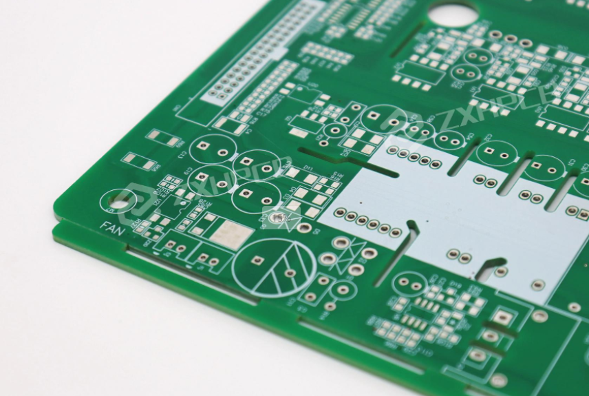
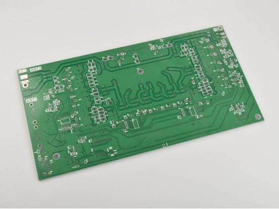
Printed Circuit Boards (PCBs) are the backbone of modern electronics, serving as the foundation upon which complex electronic devices are built. Ensuring the quality and reliability of PCBs is crucial for the performance and longevity of these devices. This guide will outline the steps and methods commonly employed in the testing of PCB products to ensure they meet the necessary standards and specifications.
Pre-Testing Inspection
Before a PCB undergoes rigorous testing, it's important to conduct a visual inspection. This step involves checking the board for any obvious defects such as missing components, soldering issues, or incorrect placements. Automated Optical Inspection (AOI) systems can be utilized to detect these defects efficiently and accurately.
Electrical Testing Methods
Once the initial inspection is complete, the PCB should undergo electrical testing to verify its functionality. There are several methods available:
-
In-Circuit Testing (ICT): ICT involves using a test fixture (jig) to probe the board at multiple points simultaneously. This method checks for open circuits, shorts, and incorrect values of passive components like resistors and capacitors.
-
Functional Testing: In functional testing, the PCB is powered up and subjected to simulated operating conditions. The goal is to ensure that the board performs all its intended functions correctly.
-
Boundary Scan Testing (BST): BST, also known as Joint Test Action Group (JTAG) testing, utilizes dedicated pins on integrated circuits to test interconnections and components without the need for physical access to every test point.
Environmental Stress Screening (ESS)
To further ensure the robustness of PCBs, Environmental Stress Screening (ESS) is recommended. ESS exposes the PCB to extreme temperatures, vibration, and other environmental stresses to simulate real-world conditions. This helps uncover latent defects that might not be apparent under normal operating conditions.
Final Quality Assurance (QA) Checks
After passing through the above stages, the PCB should undergo a final QA inspection. This involves a thorough examination of the board for compliance with design specifications and any additional customer requirements. This final step ensures that the PCB is ready for shipment or integration into a larger assembly.
Conclusion
Testing PCB products is a multi-step process that requires attention to detail and adherence to established standards. By following these guidelines, manufacturers can produce high-quality PCBs that perform reliably under a variety of conditions. Continuous improvement in testing methodologies and equipment can further enhance the efficiency and effectiveness of the PCB testing process, contributing to the advancement of electronic technologies.
If you want learn more,pls click ://sznewmeto.com
Something about ICT test jigs
Understanding PCB Test Jig Fixtures: An Essential Tool in Electronic Manufacturing
Related Article