10 interesting things about PCB: Take you into the mysteries of the electronic world

In the vast world of electronic technology, PCB (Printed Circuit Board, printed circuit board) plays a pivotal role. They are not only an indispensable part of modern electronic equipment, but also carries the important mission of connecting electronic components and transmitting electrical signals. However, about PCB, you may only know its basic definition and application, in fact, in this seemingly ordinary field, hidden many interesting and little-known stories. //sznewmeto.com/
First, the origin of PCB: from hand-drawn to automated production
PCB history can be traced back to the early 20th century, but the true meaning of PCB was invented in 1936 by the Austrian Paul Eisler (Paul Eisler). He first proposed and patented the concept of printed circuits on insulated substrates. However, due to the technological limitations at the time, the production of PCBs relied mainly on manual drawing and etching, which was inefficient and costly. It was not until the 1950s, with the rapid development of electronic technology and the introduction of automated production lines, that PCBs began to realize mass production and wide application. Today, PCB has become an indispensable part of modern electronic equipment, and its production process is increasingly sophisticated and efficient.
Second, the diversity of PCB: from single-layer boards to multilayer boards
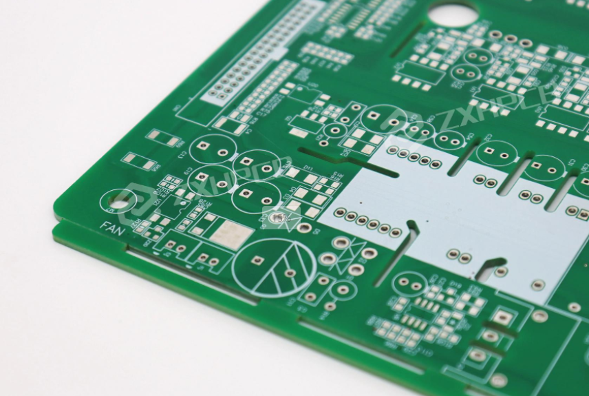
When it comes to PCB, many people may first think of a single-layer or double-layer circuit board. But in fact, there are many types of PCBs, according to the number of layers and different structures, can be divided into single-layer boards, double-layer boards, multilayer boards and flexible circuit boards. Multilayer boards are the type of PCBs commonly used in modern electronic devices, and they enable more complex and efficient circuit layouts through the interconnection of multiple conductive layers. Flexible circuit boards with its bendable, foldable characteristics, in smart phones, tablet PCs and other portable devices play an important role.
Third, the PCB on the “invisible art”: the mystery of the circuit layout
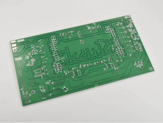
On the PCB, the layout of the circuit is not arbitrary, but after careful design and optimization of the results. Engineers need to consider the signal transmission speed, electromagnetic interference, heat dissipation and other factors to ensure the stability and reliability of the circuit. At the same time, they also need to make full use of the limited space of the PCB to achieve efficient layout of the circuit. It can be said that each piece of PCB is the crystallization of the wisdom and experience of engineers, covered with their carefully carved “invisible art”.
Fourth, PCB's “green revolution”: environmentally friendly materials and sustainable development
With the growing awareness of environmental protection, PCB industry has ushered in a “green revolution”. The traditional PCB production process uses a large number of harmful substances, such as lead, cadmium and other heavy metals, causing serious environmental pollution. To meet this challenge, the industry has begun to develop and promote environmentally friendly materials, such as lead-free solder, halogen-free solder resist, etc., to reduce the negative impact of PCB production on the environment. At the same time, through the optimization of production processes and improve resource utilization, PCB industry is striving to achieve the goal of sustainable development.
Fifth, PCB's “stealth”: cleverly hidden in the electronic equipment
In modern electronic equipment, PCB is often cleverly hidden in the internal structure, playing the role of “invisible man”. For example, in smartphones, PCB is compactly arranged on the motherboard, and a variety of chips, sensors and other components are closely linked; in the TV set, PCB is hidden behind the body or at the bottom, silently supporting the screen display and processing functions. Although they do not show, but is the cornerstone of the normal operation of electronic equipment.
Six, PCB's “transformation method”: customization and modular design
In order to meet the needs of different electronic devices, PCB shows a powerful “transformation method”. Through customized design, engineers can be based on the specific functions and requirements of the device, the flexibility to adjust the PCB shape, size and circuit layout. At the same time, modular design also makes PCB easier to produce and maintain. By breaking down complex circuits into multiple independent modules, engineers can be more efficient testing, debugging and replacement work, reducing production costs and maintenance difficulties.
Seven, PCB's “Speed and Passion”: the challenges of high-speed signal transmission and breakthroughs
In high-speed electronic equipment, PCB is facing unprecedented challenges. With the continuous increase in data transmission speed, the signal transmission delay and loss on the PCB is increasingly prominent. To meet this challenge, engineers have adopted advanced materials and technologies to optimize PCB performance. For example, the use of low dielectric constant materials as substrates can reduce signal transmission delay; the use of differential signaling technology can reduce signal interference and loss. These innovations allow PCB in high-speed signal transmission to show more excellent performance.
Eight, PCB's “light of wisdom”: the core role of intelligent electronic devices
In intelligent electronic devices such as smart phones, smart home, PCB plays a central role in the “light of wisdom”. They not only carry a variety of sensors, processors and memory chips and other components of the connection task, but also responsible for the realization of the communication between the device and data transmission. Through sophisticated circuit design and optimization, PCB for intelligent electronic devices to provide a stable and efficient operating platform, making our lives more convenient and intelligent.
Nine, PCB's “future prospects”: the exploration of new technologies and applications
With the rapid development of science and technology, PCB is also constantly exploring new technologies and applications. For example, in wearable devices, the application of flexible circuit boards makes the equipment thinner, lighter and more comfortable; in the field of Internet of Things, PCB as a bridge connecting a variety of sensors and actuators, providing the possibility of intelligent management and control. In addition, with the rise of 5G, artificial intelligence and other technologies, PCB will usher in more innovation and development opportunities.
Ten, PCB's “heroes behind the scenes”: quietly support the power of modern science and technology
Behind the bright and shiny modern technology, PCB has always played the role of “hero behind the scenes”. Although they are not as eye-catching as smart phones, tablet PCs and other end products, they are the key to the normal operation of these products. From aerospace to medical equipment, from communications equipment to industrial control, PCBs are ubiquitously supporting the development of modern technology.
What is PCB? In which fields is it applied?
Various PCB pads, have you used them all?
Related Article