PCB design and ICT testing
2024-09-21
PCB design and ICT online testing
One: Preface
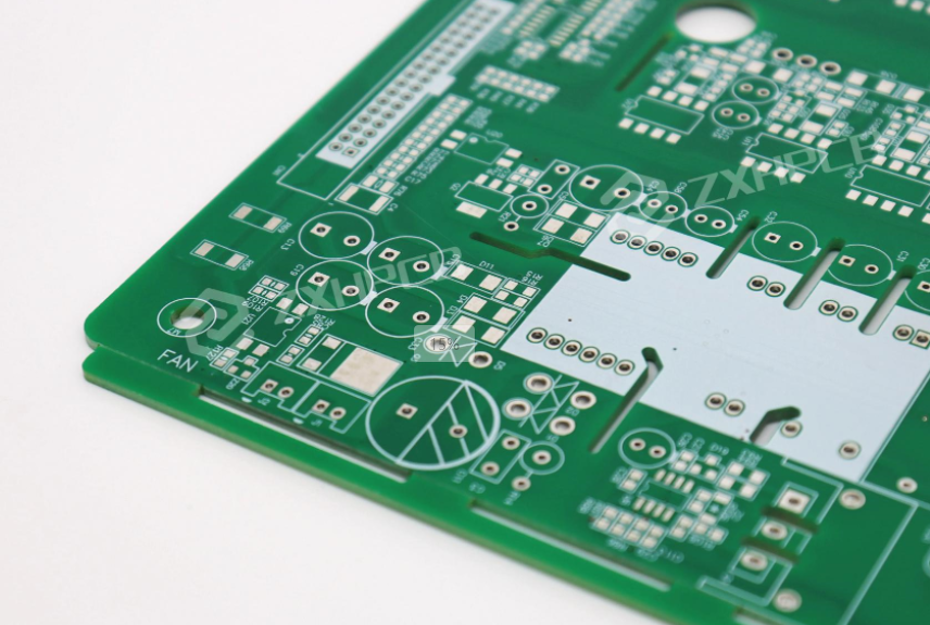
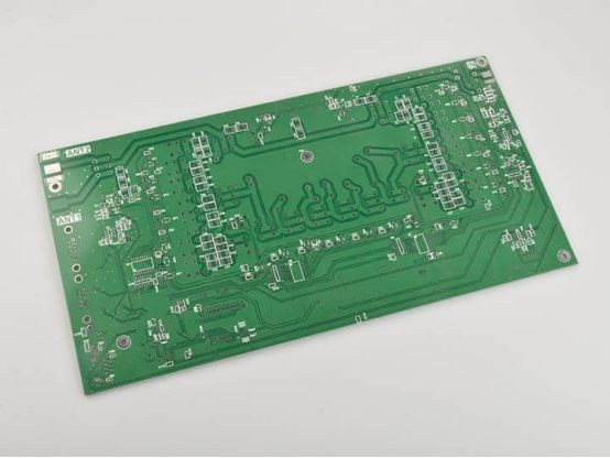
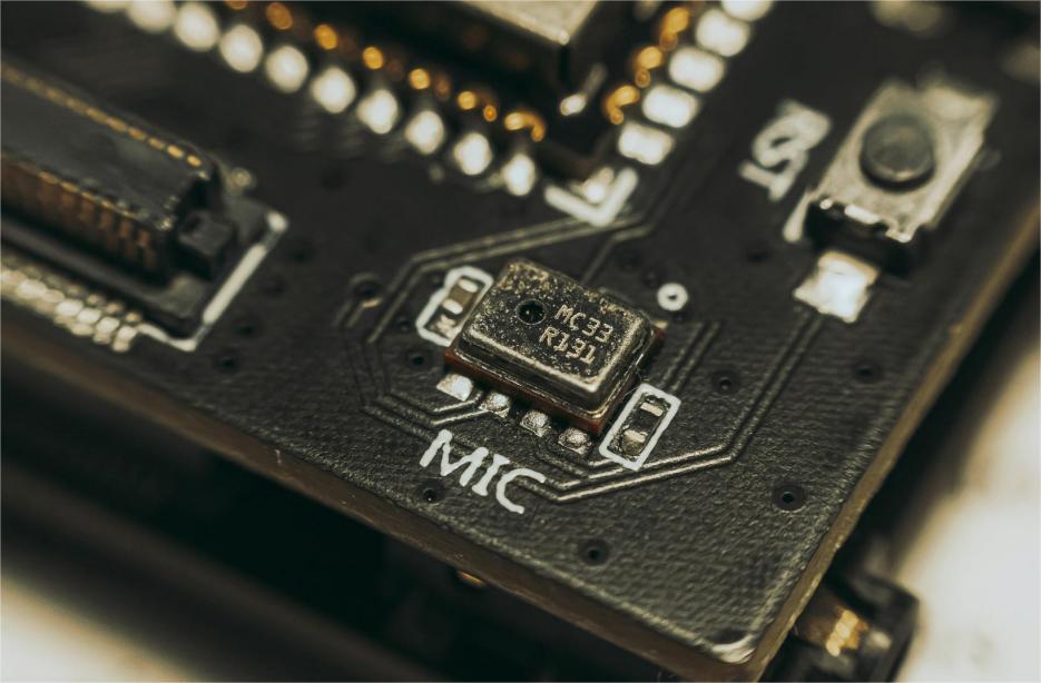
Today's electronic products are thinner and shorter, and the design and wiring of PCB is becoming more complex and difficult. In addition to functionality and safety, it needs to be producible and testable. The rules for testability requirements are provided for the reference of design and wiring engineers. If they can be paid attention to, they will save your company considerable ICT fixture production costs and improve the reliability of the test and the service life of the ICT fixture.
Two: Applicable rules
1, although there are double-sided ICT fixtures, it is best to place the measured points on the same side.
2, the priority of the measured points: A. Testpad B. Component Lead C. Through hole (Via)
3, the distance between the two measured points or the center of the measured point and the pre-drilling shall not be less than 0.050" (1.27mm). Preferably greater than 0.100" (2.54mm), followed by 0.075" (1.905mm)
4, the measured point should be at least 0.100" from its nearby parts (located on the same side), if it is higher than 3m/m parts, it should be at least 0.120".
5, the measured points should be evenly distributed on the PCB surface to avoid high local density.
6, the diameter of the measured point should be no less than 0.035"(0.9mm), such as on the needle plate, it is best not less than 0.040"(1.00mm), the shape of the square is better (the measurable area is 21% more than the circle). Points less than 0.030" need additional processing to guide the target.
7, the Pad and Via at the measured point should not be Solder (Solder Mask).
8, the measured point should be at least 0.100" from the edge or hem of the plate.
9, PCB thickness should be at least 0.062"(1.35mm), thickness less than this value of PCB easy to bend, need special treatment.
10, the diameter of the positioning Hole should be 0.125"(.3.175mm). The tolerance should be "+0.002"/-0.001". Its position should be opposite to the PCB.
11. The tolerance from the measured point to the positioning hole shall be +/-0.002".
12, avoid placing the measured point on the SMT parts, not only can the measured area be too small, unreliable, and easy to damage the parts.
13, avoid using too long part foot (greater than 0.170"(4.3mm)) or too large aperture (greater than 1.5mm) as the measured point, need special treatment.
Three: Information required for ICT fixture production
1, Layout CAD File: For example, PCADR-->*.pdf PADSR--> *.asc
2, one empty PCB board (please note the version and serial problems)
3. One solid board to be tested
4, BOM
5. Circuit diagram
1, Layout CAD File: For example, PCADR-->*.pdf PADSR--> *.asc
2, one empty PCB board (please note the version and serial problems)
3. One solid board to be tested
4, BOM
5. Circuit diagram
Four: ICT fixture PCB LAYOUT coordination matters
1, each copper foil regardless of shape, at least one test point is required.
2, the test point location to consider the order:
3, ACI plug-in part pin is preferred as the test point.
4, copper foil exposed copper part (test PAD), but preferably tin.
5, vertical parts plug-in feet.
6. Do not Mask Through the Hole.
Five, test point diameter
Above 1.1m/m, the test effect can be achieved with the general control needle.
Below 2.1m/m, a more precise probe is required to increase the manufacturing cost.
3.PAD contact must be good.
If you wanna get more information,pls contact://sznewmeto.com/
The Application of Test Fixtures in Integrated Circuit Testing
Something about ICT test jigs
Related Article